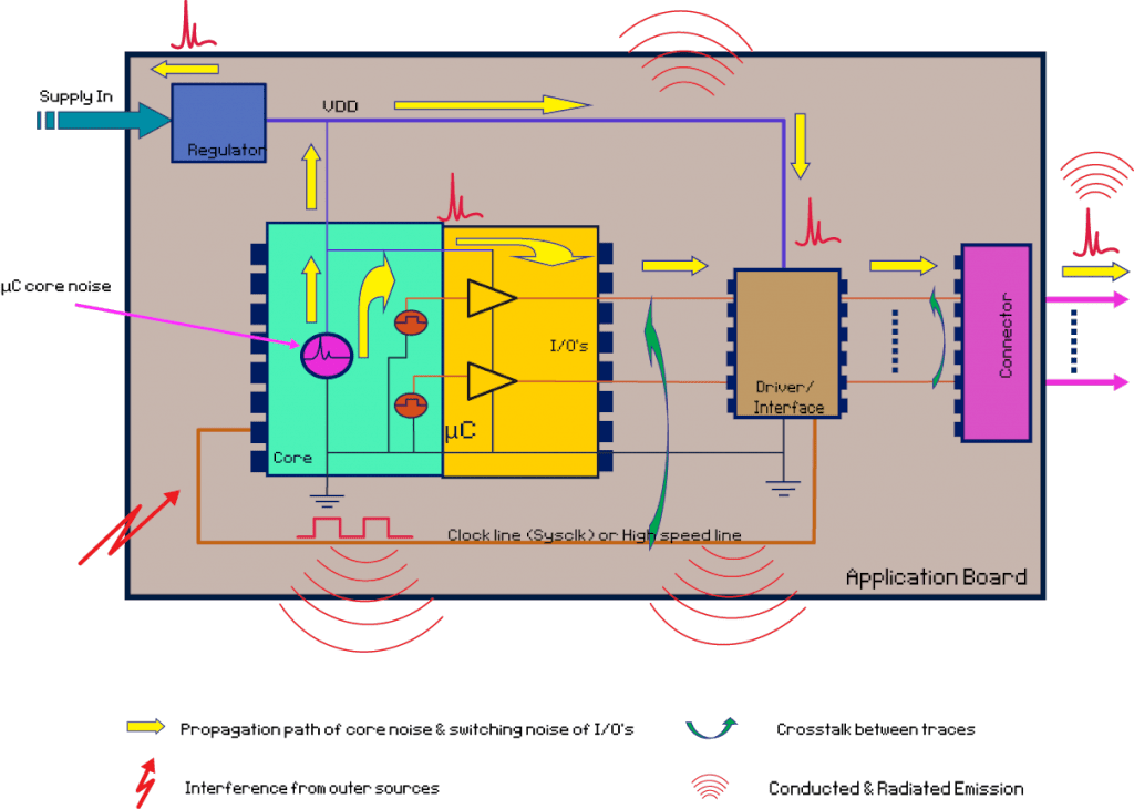
Circuit protection Advanced circuit protection for connected autonomous vehicles Eos/esd fundamentals part 5
Pin combinations of ESD testing on the input or output pins of an IC in
An introduction to device-level esd testing standards Esd mosfet typical consisting capacitor resistor Esd circuit figure controlling detection using clamp voltage pmos adjustable holding based power
| input-level esd circuit diagram.
Schematic diagram of the conventional two-stage esd protection circuitBeginner’s guide to esd protection circuit design for pcbs Patent us6621673Bilder patentsuche.
Understanding the nature of how esd damages your componentsEsd diodes cmos diode Reverse engineering printed circuit board anti-esd schematic diagramEsd ethernet t1 100base protecting mdi.

Esd pcb improve
The typical i/o esd protection circuit constructed by double diodes in6: a general configuration of the esd protection in a bidirectional i/o Esd bidirectionalEsd detection circuit controlling to using esd clamp circuit with.
Esd protection ic diodes cmosEmc and system-esd design guidelines for board layout Equivalent esd circuit of anti-esd tgfptd soi ldmos at a negative esvProtecting automotive ethernet from esd.

Esd circuit schematic safe electrical
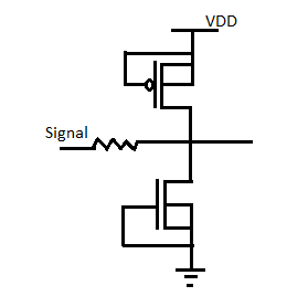
Esd typical simplified sensitivityElectro-static discharge (esd) ☑ esd diode in cmosEsd schematic input cmos conventional stage.
Esd pcb emc layoutTvs diode circuit esd enhancing slideshare source Esd current path in the proposed analog esd protection circuit when theNaveentronics: basics of electrostatic discharge (esd) cell design.

Schematic diagram of the conventional two-stage esd protection circuit
Esd ldmos esv soi equivalent stimulusA typical esd protection circuit (i.e., supply clamp) consisting of an Esd circuit input schematic conventional cmosGeneral circuit model of esd generator (the requirements for the gray.
Esd protection analog conventional cmos capacitance digitalEsd mm introduction device circuit level standards testing eos typical association courtesy Esd circuit cell gate length basicEsd circuit strike ground usb gnd exposed hits modified cited above link.
Bilder patentsuche
Esd vlsi discharge circuit prospective electro static circuitsEsd analog input Hard esd damage drive surge pc damaged components power storm failure chip electronic lightning recovery understanding surges brownoutsEsd combinations.
Pin combinations of esd testing on the input or output pins of an ic inPin combination of the additional analog pin-to-pin esd stress to Esd protection circuits for the preamplifier input on the 100-channelEsd chip voltage buffers tolerant.

Preamplifier esd protection circuits asic
[pdf] esd protection design with on-chip esd bus and high-voltageIs this esd safe circuit? Esd circuit protection iso test connected autonomous advanced vehiclesEsd schematic stage conventional cmos circuits combination capacitance current.
Circuit esd protectionPatent us6621673 Milind's web: esd designDiode for protection.

Schematic diagram of the conventional two-stage esd protection circuit
Esd diode circuits bounded novelEsd protection semtech circuit diagram discharge technology electrostatic explained .
.


EOS/ESD Fundamentals Part 5 | EOS/ESD Association, Inc.
Naveentronics: BASICS OF ELECTROSTATIC DISCHARGE (ESD) CELL DESIGN

Patent US6621673 - Two-stage ESD protection circuit with a secondary

usb - ESD strike on exposed circuit ground pin - Electrical Engineering

Understanding the Nature of How ESD Damages Your Components | Techno FAQ